Why does the semiconductor industry use bidirectional polyimide film
Bidirectional polyimide film (BOPI) has become an irreplaceable key material in semiconductor manufacturing, packaging, and testing due to its comprehensive properties such as heat resistance, high insulation, ultra stable size, radiation resistance, and flexibility, especially in the fields of process, high-density packaging, and flexible chips.
Bidirectional polyimide film (BOPI) has become an irreplaceable key material in semiconductor manufacturing, packaging, and testing due to its comprehensive properties such as heat resistance, high insulation, ultra stable size, radiation resistance, and flexibility, especially in the fields of process, high-density packaging, and flexible chips.
1、 Ultra high temperature resistance, suitable for semiconductor high-temperature processes
Semiconductor manufacturing involves multiple high-temperature processes such as diffusion, photolithography, etching, ion implantation, metallization, and bonding, with temperatures often ranging from 200 ℃ to 400 ℃.
BOPI can work stably for a long time from -269 ℃ to+260 ℃, and its short-term temperature resistance can reach over 400 ℃.
It does not melt, deform, release gas, or release harmful substances at high temperatures, and does not contaminate the wafer and cavity.
Ordinary plastic films (PET, PEN, etc.) soften and fail above 150 ℃, making them unusable.
2、 Extremely stable size ensures chip accuracy
Semiconductors require dimensional and positional accuracy to reach the micrometer or even nanometer level, and materials can be scrapped with slight deformation.
Biaxially oriented BOPI molecules have a high degree of orientation and a low coefficient of thermal expansion (CTE), making them compatible with silicon wafers, ceramics, and metal frames.
Under high temperature, the thermal shrinkage rate is less than 0.1%, and there is no warping or expansion after repeated cold and hot impacts.
Ensure zero deviation in photolithography alignment, wire bonding, flip chip packaging, and micro bump processes.
3、 Excellent electrical insulation performance ensures device reliability
Semiconductor chips have low voltage and high current density, and once the insulation fails, it will break down and burn out.
High breakdown field strength of 200-300 kV/mm
The volume resistivity reaches 10 ¹⁶~ 10 ¹⁷Ω· cm
Maintain stable insulation in high temperature and high humidity environments
Suitable for:
Wafer protective layer
Power device isolation layer
Multi layer wiring interlayer insulation
High voltage IGBT and MOSFET insulation support
4、 Resistant to radiation and chemical corrosion, suitable for harsh manufacturing environments
1. The semiconductor production line has:
High energy rays (gamma rays, electron beams)
Strong acid, strong alkali, organic solvent
Plasma etching environment
2.BOPI:
Excellent radiation resistance, no aging, no breakage
Resistant to most organic solvents and acids
Strong stability in plasma environment
Can be used as a wafer protection film, photolithography support film, and etching shielding film.
5、 High mechanical strength, ultra-thin and flexible
Semiconductors pursue thinning, lightweighting, and flexibility:
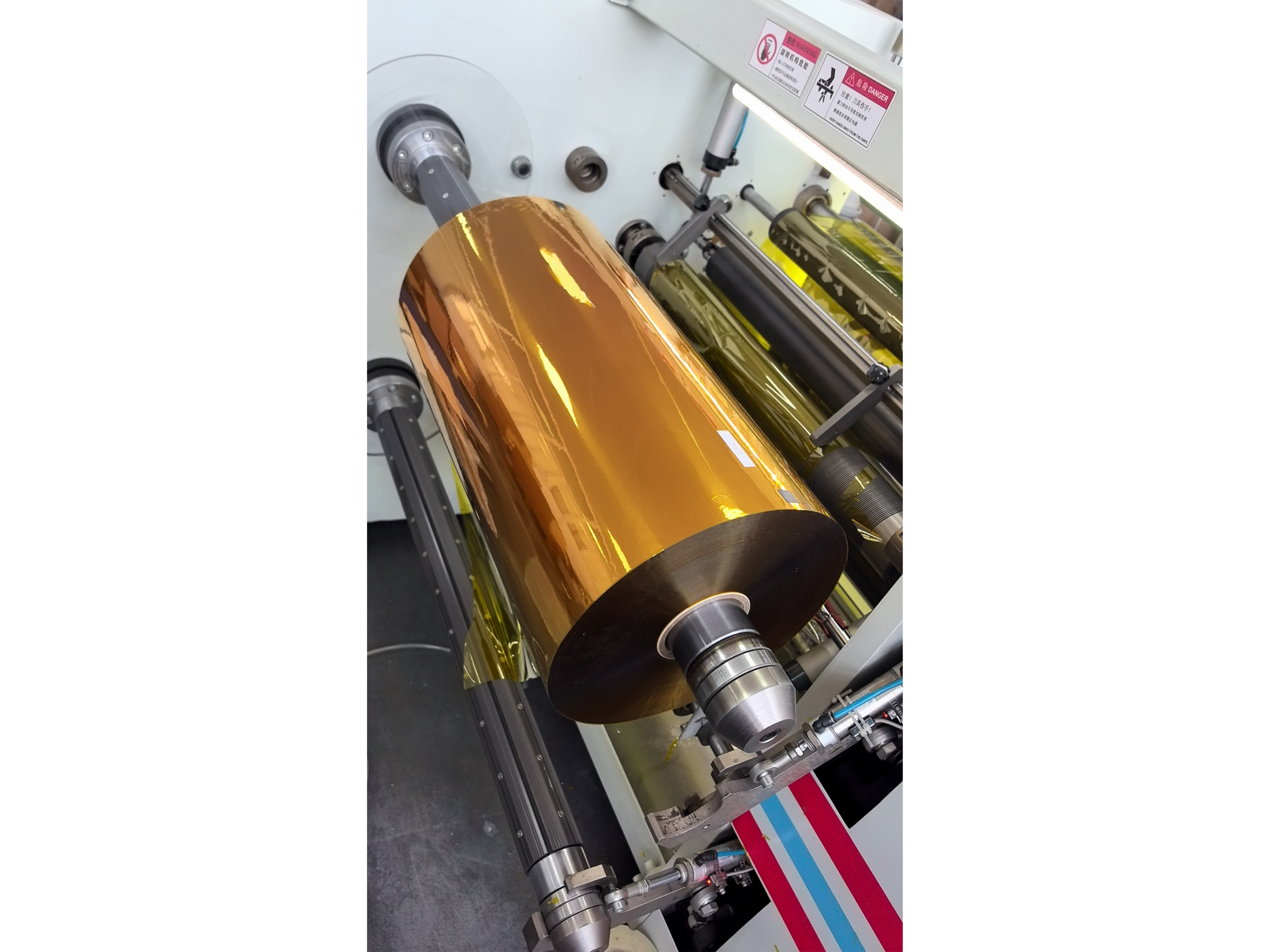
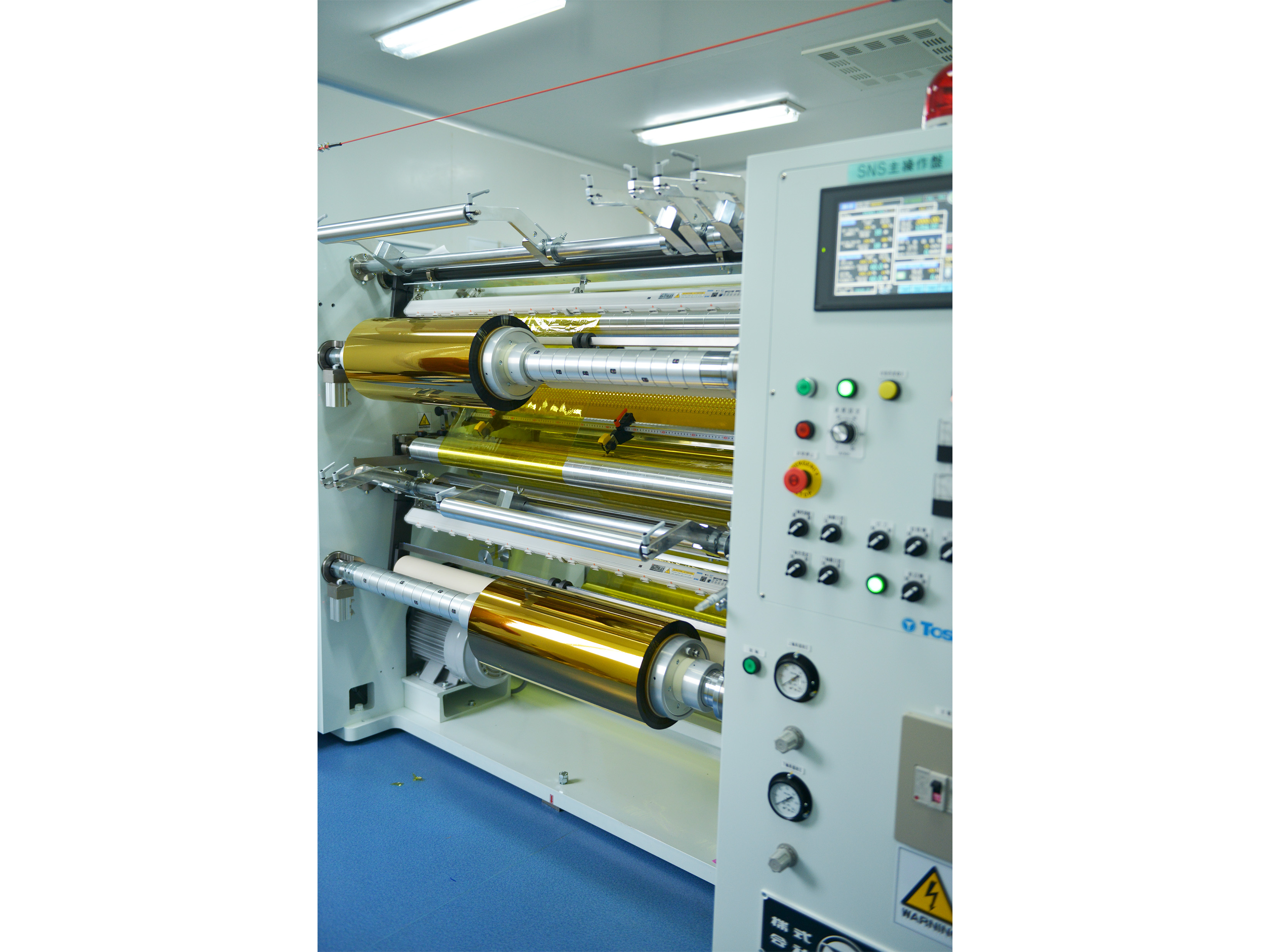
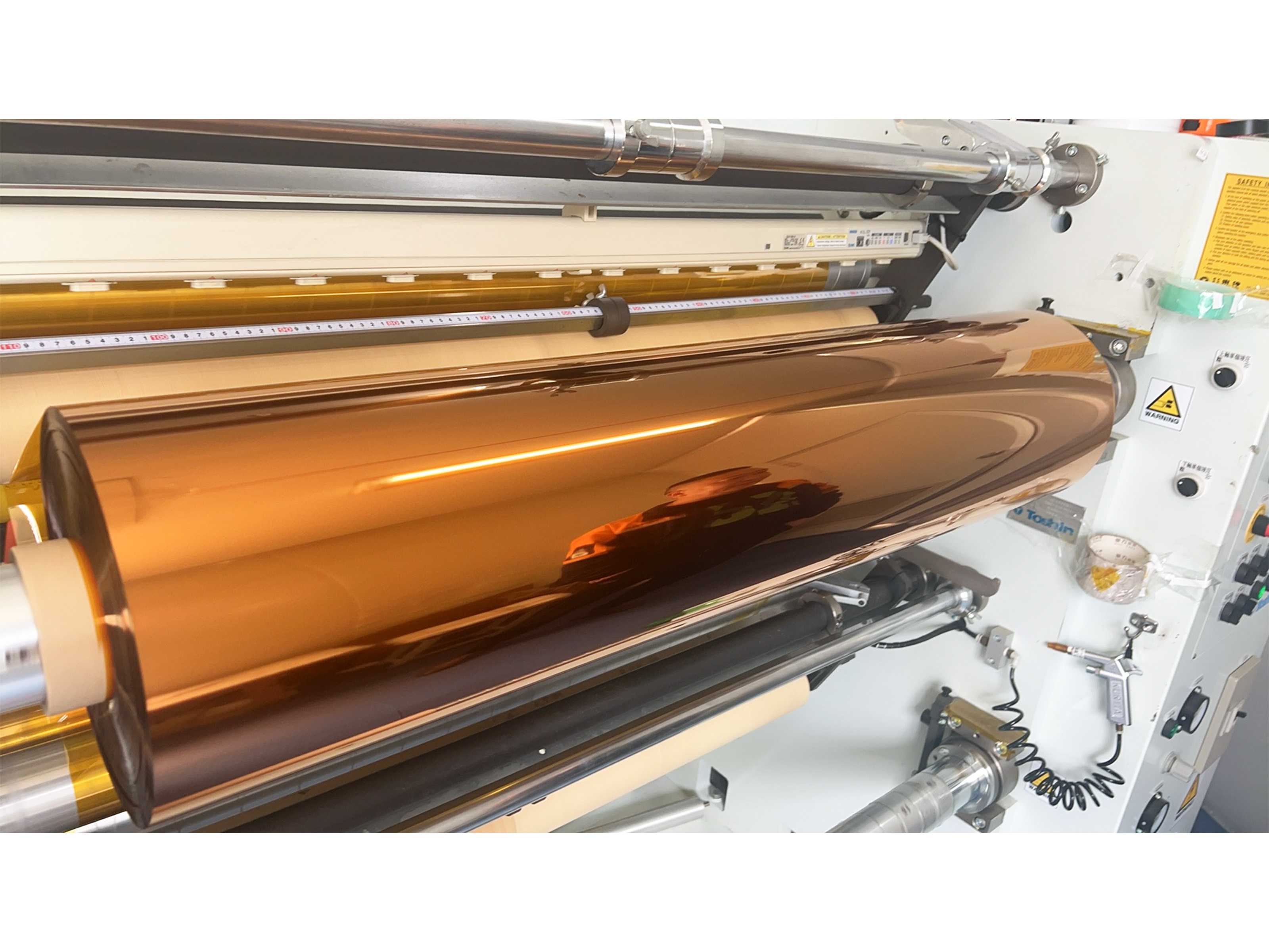
BOPI can achieve ultra-thin thickness of 12.5 μ m to 50 μ m
High tensile strength, tear resistance, and bending resistance
Curlable and foldable, supporting flexible chips, flexible sensors, and foldable screen driver ICs
It is the core substrate for wafer thinning, ultra-thin packaging, and COF/FOF.
6、 Adapt packaging technology (semiconductor core requirements)
In packaging such as Bumping, WLP, Fan out, 2.5D/3D, TSV, etc.:
Used as a chip buffer layer and stress relief layer
Reduce warpage and cracking caused by thermal mismatch between silicon wafers and substrates
Improve the reliability of flip chip (FC) and copper pillar bumps
As a dielectric material for the rewiring layer (RDL)
Without BOPI, it is difficult to achieve high-density, high reliability, and thin packaging.
7、 Low moisture absorption, high cleanliness, in line with semiconductor cleanliness requirements
BOPI has a low water absorption rate and does not precipitate or produce bubbles at high temperatures
High purity, low metal ion precipitation, does not contaminate the wafer
Meet the cleanroom usage standards of Class 10-1000 for semiconductors


 WeChat number:
 Home
Home
 Product
 Wechat
 Telephone